
Qualcomm Unveils Snapdragon Reality Elite Chip for Next-Gen AR and XR Headsets
June 16, 2026
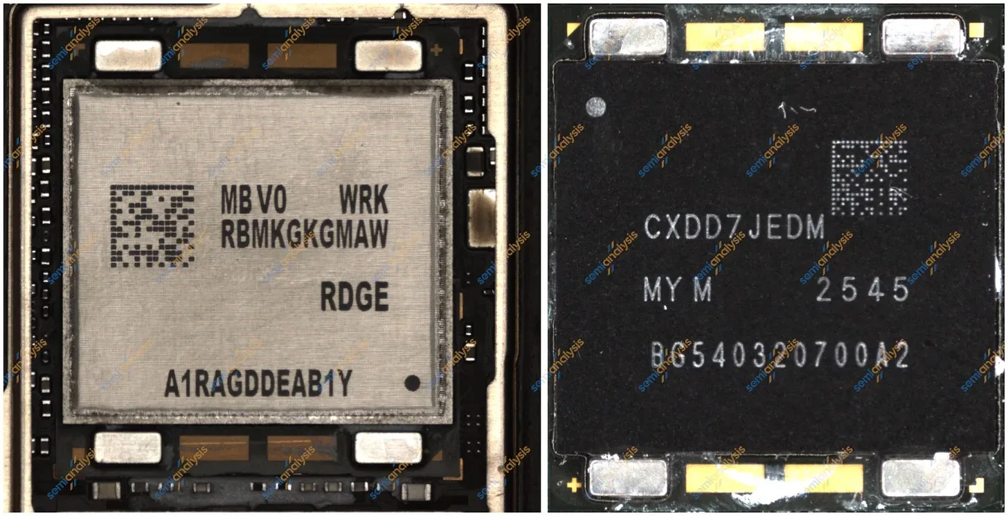
Recent investigative work by semiconductor analysts at SemiAnalysis has provided new insights into the capabilities of China’s leading contract chipmaker, Semiconductor Manufacturing International Corporation (SMIC). Utilizing a newly established reverse engineering laboratory, the firm examined the HiSilicon Kirin 9030 processor, which powers the Huawei Mate 80 smartphone series. This processor is produced using SMIC’s N+3 manufacturing node, representing the company’s third iteration of its 7-nanometer (nm) class technology.
The reverse engineering study focused on transistor density, a crucial metric in assessing the efficiency and advancement of semiconductor manufacturing processes. According to the analysis, SMIC’s N+3 technique achieves transistor density figures comparable to those of Taiwan Semiconductor Manufacturing Company’s (TSMC) N6 process, a well-regarded 6-nanometer technology widely used across the industry.
This finding is significant as it positions SMIC’s process technology in close competition with one of the most advanced semiconductor foundries globally. Achieving transistor density on par with TSMC’s N6 node indicates a substantial stride in the quality and miniaturization of chips produced domestically in China, narrowing the gap with international leaders.
Furthermore, the analysis highlighted notable achievements in the processor’s wiring layout. SMIC’s approach was found to be competitive with Intel’s 18A node, an advanced manufacturing process from the US-based semiconductor giant. This comparison suggests that while transistor density levels are still catching up, the company is showing innovation and progress in other critical aspects of chip fabrication such as interconnect design and layout efficiency.
The HiSilicon Kirin 9030 processor’s use of the N+3 process marks an important milestone in the broader development of Chinese semiconductor technology. It reflects ongoing efforts to refine and enhance local supply chains for high-performance mobile processors amid global industry challenges and geopolitical pressures.
While detailed technical specifications, market availability, and pricing for devices using the N+3 process were not disclosed, the analysis underscores the increasing sophistication achieved by SMIC’s manufacturing capabilities. This progress may impact both domestic and international markets as China continues to invest heavily in semiconductor research and production infrastructure.
Industry observers will be watching future developments closely to assess how rapidly SMIC can further mature its technology nodes and whether it can maintain momentum toward matching or surpassing competing fabs’ capabilities. For now, the newly revealed parity with TSMC’s N6 node on transistor density marks a meaningful benchmark for the company and the Chinese semiconductor ecosystem overall.
New analysis reveals SMIC’s N+3 process matches TSMC’s N6 in transistor density, highlighting advancements in Chinese chip manufacturing technology.