
Vivo X300 E Launches Soon with Zeiss Optics and Massive 7200mAh Battery
July 20, 2026
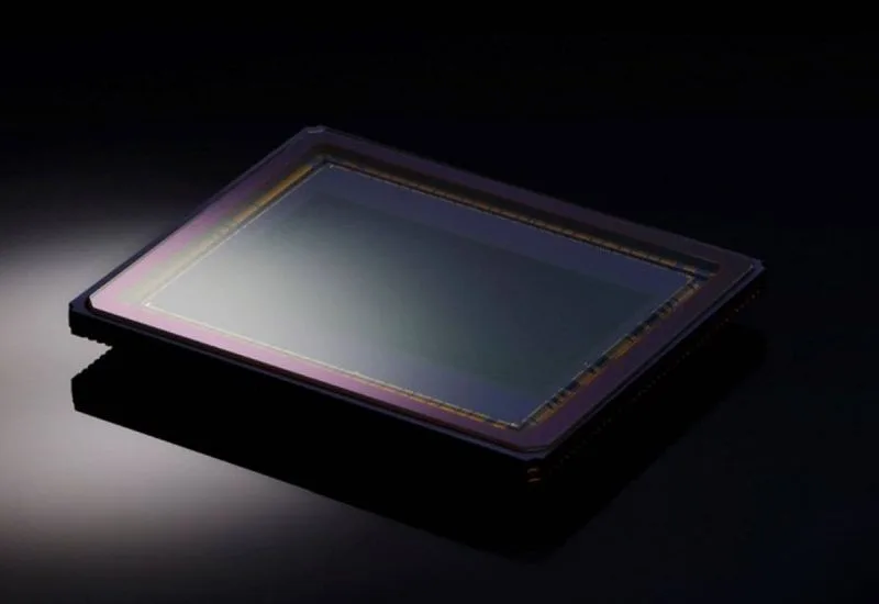
Canon is set to adopt a 2-nanometer (nm) semiconductor fabrication process developed by Rapidus for its image sensors, signaling a significant change in how these components could be manufactured in the future. This move stands out as an unusual departure from the traditional industry practice, as image sensors used in digital cameras have historically not required such cutting-edge manufacturing technologies.
For decades, companies producing image sensors have relied on more mature lithography nodes. Sony, a dominant player in the image sensor market, has long utilized a 28-nm process technology, which has proven effective and cost-efficient. Notably, Sony also participated financially in establishing TSMC’s first semiconductor fabrication facility in Japan, emphasizing local production with this established technology node.
Rapidus, a new competitor in the semiconductor manufacturing arena, offers a 2-nm process technology that represents one of the most advanced lithography scales currently under development. Canon is expected to become one of Rapidus’ initial clients, obtaining locally produced chips fabricated at this cutting-edge node. However, the rationale behind choosing such an advanced and complex process for image sensors remains unclear within industry circles.
The choice to pursue 2-nm chip production reflects Canon’s broader strategic efforts to enhance its technological capabilities and potentially reduce reliance on external suppliers for key components. However, the increased complexity and cost associated with leading-edge semiconductor manufacturing typically apply to processors and memory devices, where performance gains and power efficiency are critical.
Image sensors generally do not demand such sophisticated lithographic techniques due to their specific design requirements and performance profiles. Consequently, the practical benefits of transitioning to a 2-nm process for imaging components are subject to scrutiny among market analysts and technology experts.
Beyond technological motivations, Canon’s partnership with Rapidus may also be driven by economic and geopolitical factors, including a desire to strengthen Japan’s semiconductor production ecosystem. Rapidus’ local manufacturing capacity may offer advantages in supply chain security and national technological autonomy, areas increasingly prioritized by major electronics corporations.
While more details on Canon’s plans and the exact applications for 2-nm image sensors remain forthcoming, the development raises broader questions about the future trajectory of semiconductor fabrication in imaging technology and the evolving strategies of industry leaders in responding to competitive and market pressures.
Canon aims to source 2-nm chips from Rapidus for image sensors, marking a shift from traditional manufacturing approaches.