Vivo X300 E Launches Soon with Zeiss Optics and Massive 7200mAh Battery
July 20, 2026

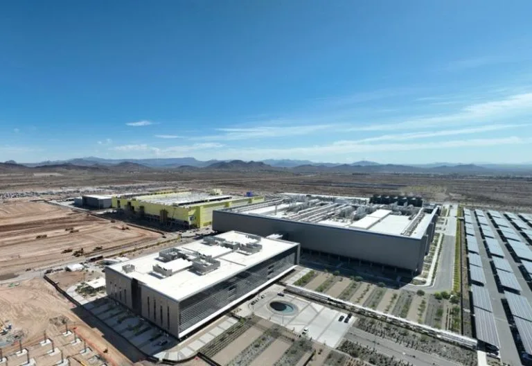
Intel is progressing in its semiconductor manufacturing with the ongoing production of its 18A process node and simultaneous development of a refined version known as 18A-P. This advancement represents a new step toward enhancing both the speed and energy efficiency of its chips while addressing thermal performance.
The 18A technology, named after its approximate 1.8-nanometer scale classification, currently serves as a key foundation for Intel’s latest chip fabrication efforts. Building upon this, the company is introducing the 18A-P variant, designed to deliver improvements in overall efficiency and heat dissipation.
Intel plans to transition 18A-P into production within the coming quarters. Although specific technical details and manufacturing timelines have not been fully disclosed, the focus on faster operation and reduced thermal output suggests an emphasis on delivering higher performance client and server processors with better energy profiles.
This approach aligns with Intel’s broader strategy to compete in the semiconductor industry by enhancing the scalability and reliability of its leading-edge process nodes. The improvements in thermal management are particularly notable, as they may contribute to better sustained performance under demanding workloads.
The 18A node itself marks a continuation of Intel’s effort to shrink transistor dimensions to the sub-2nm realm, addressing challenges in power leakage and electron flow control. The enhanced 18A-P process aims to build on this foundation with refinements that could support faster switching speeds while maintaining or improving power efficiency.
Overall, Intel’s work on the 18A and 18A-P technologies represents a critical advancement as the company seeks to maintain its competitiveness amid evolving market demands for high-performance and energy-conscious computing solutions.
Intel prepares to ramp up production of its 18A node and introduces the upgraded 18A-P process with improved performance and thermal management.