App Store Sees Surge in New Apps Amid Growth of No-Code Platforms in Early 2026
July 21, 2026
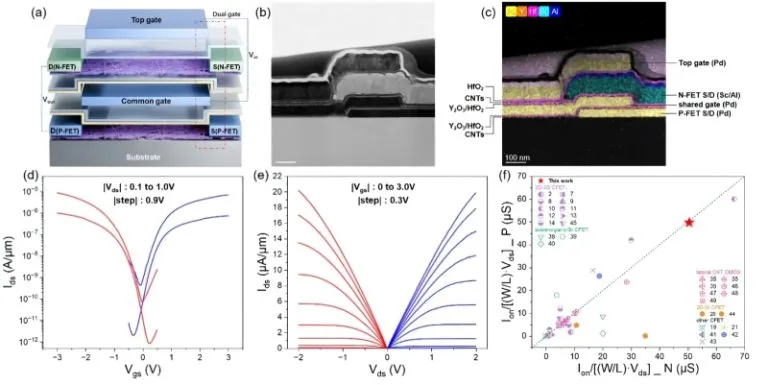
Kioxia, the Japanese memory technology company and successor to Toshiba’s semiconductor division, has revealed a novel approach to boosting NAND flash memory performance without increasing the number of memory layers. This development signals a strategic shift in addressing challenges within the competitive landscape of flash storage.
Since its invention by Toshiba in 2007, three-dimensional (3D) NAND flash memory has primarily relied on stacking multiple layers of memory cells to increase storage density. However, recent trends in manufacturing have shown that simply adding more layers faces diminishing returns and escalating complexity. Kioxia’s latest innovation seeks to overcome these limitations by employing a unique wafer bonding technology that connects silicon substrates rather than depending solely on layer count.
Rather than continuing to increase the vertical stacking of memory cells, this wafer bonding method allows Kioxia to integrate multiple wafers at the silicon level. This approach aims to enhance data density and overall memory capacity while potentially simplifying manufacturing challenges related to process yields and structural integrity.
This technology could offer significant benefits in terms of endurance and performance by optimizing the interconnection of memory cells on a horizontal scale instead of a vertical one. While competitors continue pushing for higher layer counts, Kioxia’s solution proposes an alternative pathway to remain competitive without the traditional trade-offs associated with ultra-high stacking.
The specific technical details and implications on production costs, power efficiency, and speed have not been disclosed. However, this shift highlights the company’s commitment to innovation in the flash memory sector amid increasing demands for higher capacity and reliability, especially for applications spanning from consumer electronics to enterprise storage solutions.
As semiconductor manufacturers face physical and economic challenges tied to further miniaturization and layer count extension, Kioxia’s wafer bonding technology could represent an important step in the evolution of NAND flash memory architecture. Integrating multiple wafers could open new design possibilities and pave the way for next-generation solid-state drives and memory devices.
The broader industry will be watching how this approach performs in real-world applications and whether it can offer a sustainable advantage over conventional methodologies that are approaching material and fabrication limits.
Kioxia aims to compete in the NAND flash market by enhancing memory density through wafer bonding instead of adding more layers.