
Russian Company Launches Second Batch of Satellites for Domestic Starlink Alternative
July 20, 2026
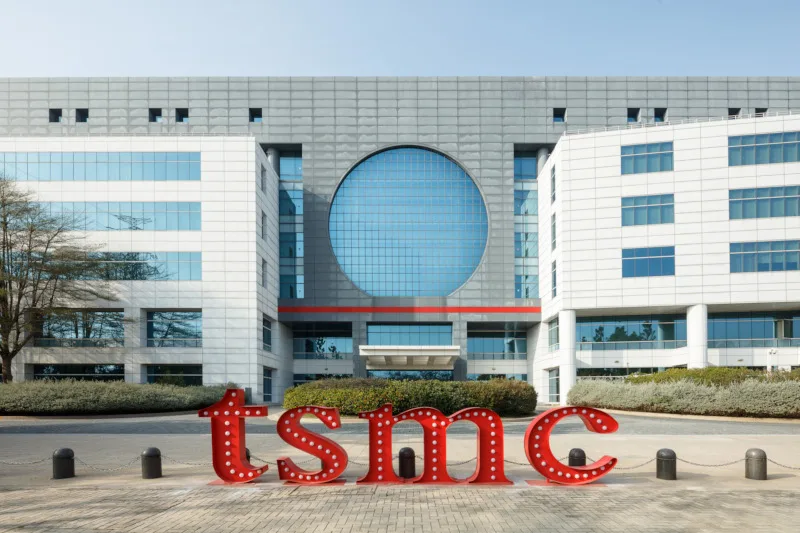
TSMC, the world-leading semiconductor foundry, is preparing to begin experimental production of chips using its new subnanometer A10 process technology by 2029. This development was outlined during a recent financial briefing where the company also disclosed its ongoing investments and production plans.
During the briefing, TSMC’s CEO, C.C. Wei, revealed that the company’s established 3-nanometer (3nm) node already accounts for a significant portion of their revenue, contributing 25 percent in the first quarter. The strong performance of 3nm chips underscores TSMC’s dominance in advanced semiconductor manufacturing and sets the stage for the next generation of process technology.
TSMC plans to ramp up its manufacturing capabilities for 3nm technology through new production facilities in Taiwan, the United States, and Japan, anticipated to come online between 2027 and 2028. These expansions aim to meet growing global demand for chips in sectors such as smartphones, high-performance computing, and AI-driven applications.
Looking beyond 3nm, TSMC is developing the subnanometer A10 process, which targets further scaling down transistor sizes and improving energy efficiency and performance on advanced chips. The company intends to commence experimental runs of A10 chips by 2029, signaling its commitment to maintaining technological leadership in the semiconductor industry.
The introduction of the A10 process aligns with broader industry trends where manufacturers pursue new materials and innovative techniques to continue Moore’s Law-like progress as traditional scaling becomes more challenging.
Additionally, TSMC mentioned plans to incorporate its CoPoS (Chip on Package on Substrate) technology in the upcoming fabrication processes. CoPoS provides enhanced integration capabilities by stacking multiple chip components in a compact design, which can boost performance and reduce latency in complex chip architectures.
TSMC’s strategic investments in advanced manufacturing nodes and cutting-edge packaging technologies demonstrate its focus on staying at the forefront of semiconductor innovation. This is crucial as demand for more powerful and efficient chips intensifies amid the expanding adoption of artificial intelligence, 5G, and next-generation computing devices worldwide.
While specific details regarding production scale, commercial availability, or pricing of the A10 process were not disclosed, the company’s roadmap clearly indicates a sustained effort to push process technology well into the next decade.
TSMC’s efforts in expanding global fabrication capacity and pioneering new nodes underscore its vital role in supporting the semiconductor supply chain, which is essential for technological advancement across numerous industries.
TSMC plans to initiate trial manufacturing of chips using its subnanometer A10 process by 2029, aiming to advance beyond current 3nm technology.