Popular PC Components in Russia Highlight Nvidia RTX 50 Series and 1TB NVMe SSDs
July 21, 2026
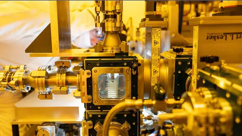
Extreme Ultraviolet (EUV) lithography remains a crucial technology in semiconductor manufacturing, balancing the need for both high precision and fast processing times when transferring circuit patterns onto silicon wafers. Conventionally, efforts to enhance the throughput of EUV scanners have focused on increasing the radiation source power or improving the sensitivity of the photoresist materials used. However, both approaches face significant technical obstacles.
A team of researchers at Imec, a leading Belgian research institute specializing in nanoelectronics and digital technologies, has identified an unexamined avenue that could improve the performance of EUV lithography systems. This discovery offers a potential increase in the speed of pattern transfer during chip fabrication without the need to escalate the radiation power or alter photoresist sensitivity.
According to the researchers, the image transfer process involves a delicate trade-off between pattern fidelity and throughput. Increasing source power to speed up exposure comes with challenges such as thermal management and source stability, while enhancing photoresist sensitivity may compromise resolution and processing reliability. The newly proposed concept addresses these limitations by optimizing other aspects of the lithography process.
While specific technical details remain to be disclosed, the approach presents a promising direction that had not been previously considered in the industry. By focusing on this overlooked parameter space, Imec’s researchers believe that the semiconductor manufacturing cycle time could be substantially reduced, accelerating the production of advanced microchips.
The innovation could be particularly impactful as the semiconductor sector continues to push towards smaller node sizes and higher complexity devices, where EUV lithography is essential. Improving scanner throughput without the costly redesigns of source or resist components may provide a more practical and scalable means of advancement.
Imec’s findings highlight the ongoing importance of fundamental research in addressing challenges in semiconductor fabrication. As chipmakers face increasing demand for faster and more efficient manufacturing processes, incremental yet practical improvements like this may play a critical role in maintaining progress within the industry.
Further studies and validation are anticipated to assess the full scope and implementation feasibility of this discovery. If successful, the industry may see new standards and techniques emerge to complement existing EUV scanner technologies, ultimately enabling higher production yields and shorter lead times in chip manufacturing.
Scientists at Belgium’s Imec discover an innovative method to enhance EUV scanner throughput without increasing source power or resist sensitivity.