Tag: photolithography
Exploring the Future of High-NA EUV Photolithography Beyond Current Limits
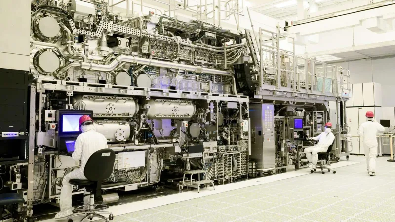
High-NA EUV photolithography at 13.5 nm currently leads semiconductor manufacturing but faces challenges in further miniaturization.
Read More
Belgian Researchers Identify New Approach to Speed Up EUV Lithography
Scientists at Belgium’s Imec discover an innovative method to enhance EUV scanner throughput without increasing source power or resist sensitivity.
Read More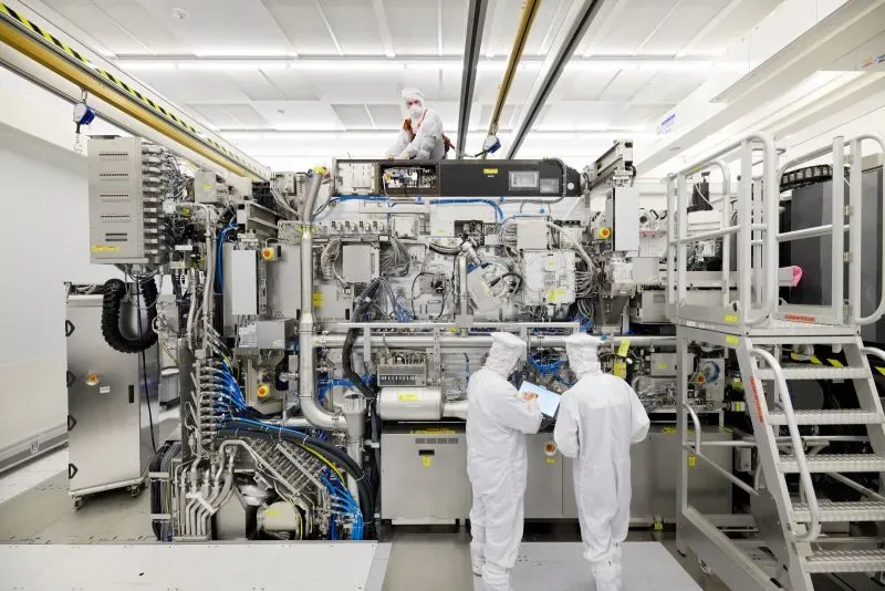
ASML Advances EUV Lithography with 1kW Light Source, Boosting Semiconductor Production by 50%
ASML enhances EUV lithography with a 1kW light source, enabling a projected 50% increase in chip production within a few years.
Read More