Advancements in CFET Technology Promise Faster, Smaller, and More Reliable Semiconductor Transistors
July 21, 2026
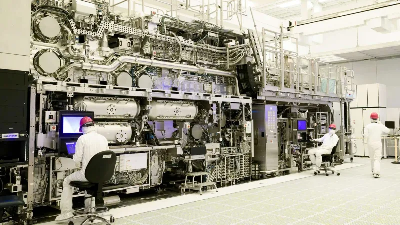
Extreme Ultraviolet (EUV) photolithography, particularly at a wavelength of 13.5 nanometers, currently represents the most advanced and widely accessible method for semiconductor manufacturing. This technology has enabled the continued trend of miniaturization in chip fabrication, allowing for increasingly dense and complex integrated circuits.
However, industry experts are now grappling with the realization that even EUV lithography at this scale might soon reach its technical limits. To sustain the momentum of semiconductor progress and achieve further reductions in feature sizes, next-generation lithographic techniques are being explored.
Among the most promising developments in the field is High Numerical Aperture (High-NA) EUV lithography, which aims to improve resolution beyond what current systems offer. Numerical aperture is a crucial parameter that influences the ability of lithographic equipment to print finer details on semiconductor wafers. Increasing the NA allows for smaller feature sizes but requires significant engineering advancements.
The current standard EUV lithography machines operate at a fixed wavelength of 13.5 nm but have inherent resolution ceilings due to their optical design and source characteristics. High-NA systems are being developed to overcome these constraints by employing larger incidence angles and more sophisticated optics. These improvements could potentially extend the life cycle of EUV technology and enable fabrication at even smaller scales, supporting future node reductions in semiconductor manufacturing.
Despite these technological strides, the deployment of high-NA EUV lithography faces various obstacles. The complexity and cost of designing and manufacturing optics that can handle higher numerical apertures are significant. Additionally, integrating such systems into existing semiconductor fab environments while maintaining throughput and yield reliability presents challenges.
The semiconductor industry is watching these technological developments closely, as the demand for smaller, faster, and more energy-efficient chips continues to rise. Innovations in photolithography directly impact the capabilities of consumer electronics, data centers, and emerging technologies such as artificial intelligence and 5G communications.
With EUV systems currently at the forefront, the exploration of high-NA EUV photolithography reflects an ongoing commitment to pushing the boundaries of nanoscale manufacturing. The next few years will be critical in determining how this technology evolves and integrates into the highly competitive and fast-moving semiconductor ecosystem.
High-NA EUV photolithography at 13.5 nm currently leads semiconductor manufacturing but faces challenges in further miniaturization.