Tag: high-na
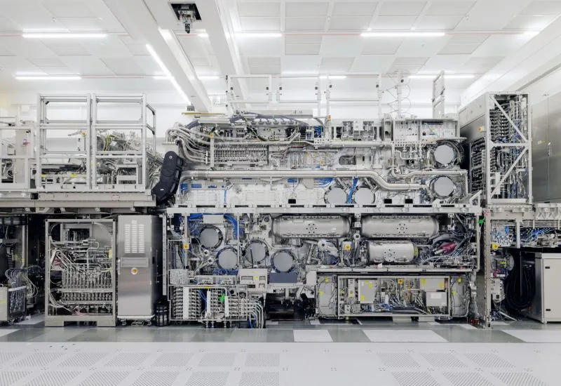
Samsung Delays Adoption of High-NA Lithography Technology Due to Costs
Samsung is holding back on incorporating High-NA lithography for chip manufacturing, citing high costs as the primary factor.
Read More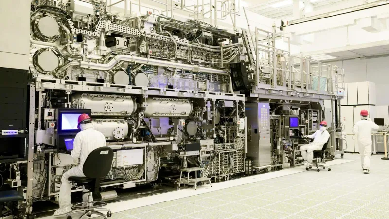
Exploring the Future of High-NA EUV Photolithography Beyond Current Limits
High-NA EUV photolithography at 13.5 nm currently leads semiconductor manufacturing but faces challenges in further miniaturization.
Read More
Intel Advances Development of Next-Gen 10A and 7A Process Technologies
Intel has initiated development of its ultra-thin 10A and 7A process nodes, with early 14-angstrom chips set for testing this fall.
Read More