Russian Company Launches Second Batch of Satellites for Domestic Starlink Alternative
July 20, 2026
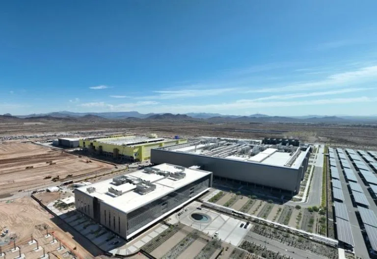
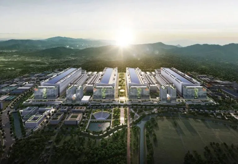
Intel has begun the development of its upcoming 10A and 7A semiconductor manufacturing process nodes, marking a significant step in the company’s roadmap for next-generation chip production. These process technologies are intended to succeed the existing 18A node and the soon-to-arrive 14A process.
The move toward 10A and 7A nodes reflects Intel’s commitment to maintaining progress in scaling and performance improvements over the next decade. These advanced nodes are expected to incorporate Extreme Ultraviolet (EUV) lithography utilizing high numerical aperture (High-NA) optics from ASML, the industry leader in semiconductor manufacturing equipment. Notably, High-NA EUV has already been implemented in the development of the upcoming 14A process, indicating a technological continuity and evolution in Intel’s manufacturing techniques.
Early samples of 14-angstrom chips fabricated using these new methods are scheduled for experimental evaluation as early as October. This milestone sets the stage for iterative refinements before mass production and broad market deployment of the 10A and 7A nodes.
Such advancements play a critical role in enhancing chip performance, power efficiency, and density, essential parameters in the evolving landscape of computing, artificial intelligence, and other high-demand applications. Intel’s continued investment in these developments showcases its efforts to sustain competitiveness amid aggressive innovation cycles in the semiconductor industry.
Details regarding specific technical improvements, launch timelines, and commercial availability for the 10A and 7A processes have not been disclosed at this time. Industry observers anticipate that information will emerge as Intel progresses through its development milestones and begins ramping test chip production.
Intel has initiated development of its ultra-thin 10A and 7A process nodes, with early 14-angstrom chips set for testing this fall.