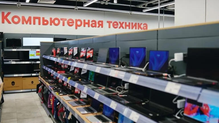
Popular PC Components in Russia Highlight Nvidia RTX 50 Series and 1TB NVMe SSDs
July 21, 2026
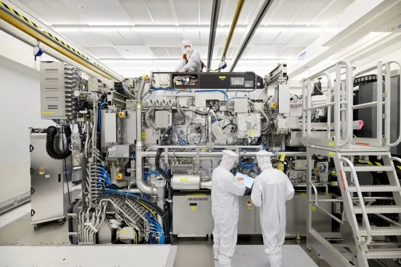
ASML, a leading manufacturer of photolithography systems for the semiconductor industry, has achieved a significant milestone in extreme ultraviolet (EUV) lithography technology. The company’s engineers have successfully increased the power of their EUV light source to 1,000 watts. This enhancement is expected to substantially improve the performance of EUV scanners.
By ramping up the light source power to one kilowatt, ASML’s EUV systems can now process silicon wafers at a much faster rate. The upgraded technology is projected to handle up to 330 wafers per hour, representing a major leap forward in chip manufacturing efficiency. This advancement is poised to reduce semiconductor production costs, particularly for leading-edge processors that rely on intricate and precise lithographic processes.
The improvement in throughput could lead to a 50% increase in chip output by the year 2030, according to ASML. As the demand for smaller, more powerful, and energy-efficient semiconductor components grows, such innovations in photolithography are critical to meeting global supply needs and advancing next-generation electronics.
ASML’s progress comes amid a highly competitive semiconductor market where manufacturers continuously seek to optimize production techniques and scale capacity. EUV lithography, which uses extremely short wavelengths of light, enables the fabrication of complex microelectronic structures that are essential for modern processors and memory devices.
Enhancements in the power and stability of the EUV light source reduce bottlenecks in wafer processing, allowing chipmakers to increase output without compromising precision or quality. ASML’s new system capabilities promise to benefit foundries and integrated device manufacturers aiming to keep pace with technological scaling and market demands.
While specific details regarding commercial deployment timelines and pricing were not disclosed, industry analysts anticipate that this innovation will ripple across the semiconductor manufacturing ecosystem. Increased productivity can translate into more affordable advanced chips and improved availability for various technology sectors, from consumer electronics to automotive and artificial intelligence applications.
ASML’s milestone underscores the ongoing evolution of semiconductor fabrication technology, aligning with broader industry ambitions to push the boundaries of computing performance and energy efficiency. As global chip demand continues to rise, breakthroughs like this will be key drivers in sustaining the momentum of Moore’s Law and enabling new classes of devices.
ASML enhances EUV lithography with a 1kW light source, enabling a projected 50% increase in chip production within a few years.