Honor Launches X7e Smartphone in Russia Featuring 7200mAh Battery and AI Shortcut Button
July 21, 2026
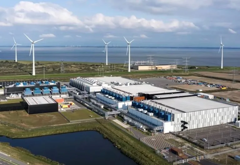
Samsung Electronics is set to expand its semiconductor manufacturing capabilities with ambitious plans to develop a 1-nanometer (nm) fabrication process by 2030. This move positions the South Korean tech giant to compete more aggressively within the contract chip production market, which is currently facing constraints due to shortages in manufacturing capacity at other leading foundries.
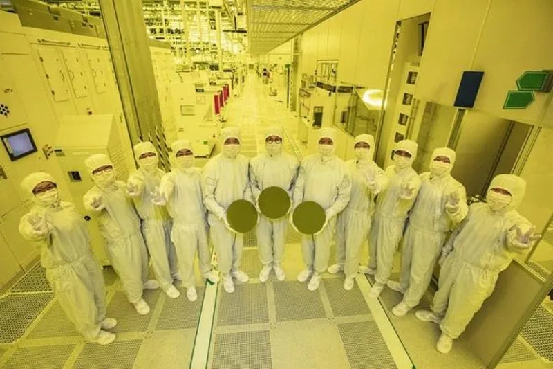
In response to the increasing demand for cutting-edge semiconductor technologies, Samsung is preparing to offer a variety of 2nm process options to its clients in the near term. These advancements are expected to deliver significant improvements in chip performance and energy efficiency, catering to a broad range of applications across the electronics industry.
Samsung’s longer-term objective entails mastering the 1nm process node, a technological milestone that presents formidable engineering and manufacturing hurdles. Achieving 1nm process technology requires overcoming physical and material limits that have increasingly challenged the semiconductor industry at such scales.
To facilitate this leap, Samsung plans to introduce a novel transistor layout featuring what it describes as “forked sheets.” This innovative architectural approach is anticipated to help maintain transistor performance and reliability as device dimensions shrink, potentially enabling continued progress in Moore’s Law scaling beyond conventional planar transistor designs.
Such a transistor design could improve electron transport and gate control, aspects critical to the operation and efficiency of next-generation chips. While details on the implementation and impact of this layout are limited, the emphasis on new transistor architectures highlights Samsung’s focus on both process technology and device innovation.
The broader context for Samsung’s strategic roadmap includes shifting dynamics in global semiconductor manufacturing. TSMC, a dominant player in the foundry market, is currently experiencing limited manufacturing capacity, creating opening opportunities for competitors like Samsung to gain market share by expanding and advancing their production technologies.
Samsung’s goal to build on its 2nm process offerings by eventually delivering a 1nm platform underlines the company’s commitment to pushing the envelope of semiconductor fabrication. This strategy aligns with the growing demand for high-performance, power-efficient chips underpinning technologies such as artificial intelligence, 5G connectivity, and advanced computing.
While Samsung continues to innovate in process nodes and device structures, specifics concerning production timelines, commercial availability, and detailed technical parameters remain forthcoming. The company’s efforts signify an important chapter in semiconductor evolution as the industry searches for new solutions to extend chip performance and scalability into the coming decade.
Samsung targets mastering 1nm chip technology and new transistor layouts by 2030 amidst growing demand for advanced semiconductor manufacturing.