Microsoft Addresses Concerns Over Xbox Staff Cuts and H-1B Visa Replacements
July 11, 2026
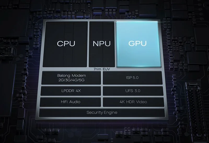
Huawei is preparing to evolve its processor designs by implementing a multilayer chip layout to significantly increase transistor density. This approach aims to improve semiconductor performance without relying on further reductions in lithography node size, a shift that represents a notable change in how chip advancement is typically achieved.
According to statements from He Tingbo, head of Huawei’s semiconductor division, the company is initially focusing on the integration of two-layer chip stacks. This multilayer configuration is expected to allow for more transistors to be packed into the same chip footprint, which could lead to enhanced processing capabilities and efficiency improvements.
Beyond the initial two-layer models, Huawei envisions expanding this technology to incorporate three or even four layers over time. This expansion will further elevate transistor density and could provide a new path for semiconductor innovation, circumventing some of the challenges associated with traditional scaling methods.
The industry has faced increasing difficulties in sustaining the pace of Moore’s Law through smaller lithography nodes, as reductions in transistor size become more complex and costly. Huawei’s strategy represents a pivot towards structural chip design innovations that focus on vertical stacking rather than purely horizontal miniaturization.
While details regarding the precise timelines, performance metrics, or specific applications for these multilayer processors remain limited, the move reflects Huawei’s commitment to advancing semiconductor technology amid global competition and evolving demands for high-performance computing.
This multilayer chip design approach aligns with broader industry trends where several companies explore three-dimensional architectures to sustain improvements in processing power and energy efficiency. By stacking transistor layers, chipmakers can increase functionality without enlarging the chip’s physical size, which is crucial for applications ranging from smartphones to data centers.
Huawei’s pursuit of multilayer semiconductors also underscores the importance of innovation in chip packaging and integration technologies, which are critical factors in managing heat dissipation, signal integrity, and manufacturing complexity when working with stacked layers.
As semiconductor technologies face physical and economic barriers to traditional scaling, Huawei’s strategy to deploy multilayer chip construction could mark a significant milestone in the chip industry’s evolution, potentially influencing how processors are developed in the coming years.
Huawei aims to enhance transistor density in processors through multilayer chip layouts, starting with two layers and potentially expanding to four.