Scientists Detect Atmosphere on Rocky Exoplanet in Habitable Zone
July 17, 2026
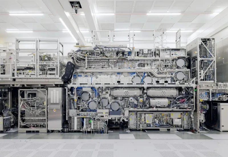
Samsung Electronics is taking a cautious approach to implementing advanced semiconductor lithography equipment known as High Numerical Aperture (High-NA) scanners. Despite being a leader in chip manufacturing technology alongside companies like Taiwan Semiconductor Manufacturing Company (TSMC) and Intel, Samsung has yet to integrate High-NA technology into its production lines due to economic considerations.
High-NA lithography represents a significant advancement in photolithography, a critical process in semiconductor fabrication that defines the intricate circuits on chips. This technology offers improved precision and resolution, enabling the production of smaller, more efficient, and higher-performing semiconductor devices. However, the equipment required to support High-NA is considerably more expensive than existing systems, prompting semiconductor giants to carefully evaluate the timing and financial impact of adopting this technology.
Intel stands out as the only major player to have started deploying High-NA lithography tools in its manufacturing operations. The company’s early move positions it as a frontrunner in pushing the technological boundaries in chip production, potentially offering advantages in next-generation semiconductor chips. Meanwhile, TSMC has communicated its perspectives on High-NA deployment but has not yet fully integrated the technology at scale.
Samsung’s executive leadership has explicitly noted that economic factors weigh heavily in the company’s decision-making regarding High-NA implementation. The prohibitive cost of acquiring and outfitting production lines with this cutting-edge equipment has contributed to its more measured approach. This financial prudence highlights the challenges semiconductor manufacturers face in balancing technological innovation with cost management, especially as demand for ever-smaller and more complex chips continues to grow.
The semiconductor industry’s cautious progression toward High-NA lithography reflects broader market dynamics and competitive strategies among the top foundries. While the promise of better chip performance and efficiency drives interest in High-NA, the substantial investment required remains a significant barrier. Samsung’s delay underscores how economic feasibility remains a dominant factor in the timing of technology adoption.
As global demand for advanced semiconductors intensifies—fueled by sectors such as artificial intelligence, 5G, and high-performance computing—the role of High-NA lithography is expected to become increasingly important. How and when Samsung and other manufacturers fully embrace this technology will have implications for the semiconductor supply chain and industry innovation trajectory.
In summary, Samsung’s reserved stance on High-NA scanner deployment is primarily a cost-driven decision, contrasting with Intel’s quicker adoption and positioning the semiconductor landscape as one to watch as companies navigate the trade-off between cutting-edge capability and financial investment.
Samsung is holding back on incorporating High-NA lithography for chip manufacturing, citing high costs as the primary factor.