Advancements in CFET Technology Promise Faster, Smaller, and More Reliable Semiconductor Transistors
July 21, 2026
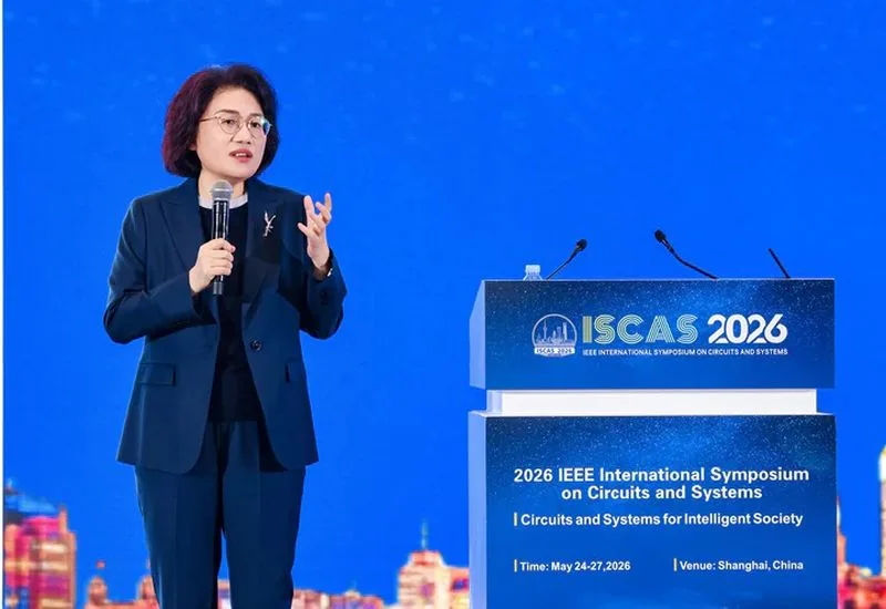
During the ISCAS 2026 conference held in Shanghai, Huawei Technologies presented an alternative strategy for advancing semiconductor chip performance that deviates from the traditional methods associated with Moore’s Law. The company outlined its ambition to close the gap with Western semiconductor manufacturers currently working on 1.4-nanometer process nodes by the year 2031.
Moore’s Law has largely driven chip evolution through the continuous shrinking of transistor sizes to pack more components into smaller areas, thereby boosting performance. However, Huawei’s researchers proposed a shift away from this geometry-centric scaling approach. Instead, they advocate for enhancing semiconductor efficiency by focusing on optimizing the timing of signal transmission within chips.
This new principle acknowledges physical and economic challenges in further miniaturizing chip structures and emphasizes the critical role that signal delay and timing optimization play in chip speed and power consumption. Huawei’s approach could redefine the pathways for semiconductor development, especially as the industry approaches limits in lithography precision and fabrication costs.
At the conference, Huawei representatives detailed how optimizing signal propagation times could serve as a pivotal method for increasing chip performance metrics without solely relying on reducing transistor dimensions. By improving the way electrical signals move across the semiconductor material, there is potential to achieve significant gains in processing speed and power efficiency, elements essential for next-generation computing and artificial intelligence workloads.
This strategy also aligns with broader industry trends exploring new materials, chip architectures, and design methodologies that complement or extend beyond the classical chip-scaling paradigm. While specifics about Huawei’s implementation or the technologies underpinning this timing optimization were not disclosed, the company’s vision marks a notable effort in the competitive semiconductor landscape.
Huawei’s initiative reflects an adaptive approach in semiconductor R&D amid geopolitical pressures and supply chain challenges. By 2031, they intend to match the performance capabilities of sub-2 nanometer technologies being developed in Western labs but through a fundamentally different optimization lens.
The announcement at ISCAS 2026 invites further attention from industry observers and competitors, as the semiconductor sector seeks sustainable innovation paths amid the slowing pace of traditional Moore’s Law improvements.
At ISCAS 2026 in Shanghai, Huawei reveals plans to surpass Moore’s Law limits by focusing on signal transmission timing to enhance chip performance.