Popular PC Components in Russia Highlight Nvidia RTX 50 Series and 1TB NVMe SSDs
July 21, 2026
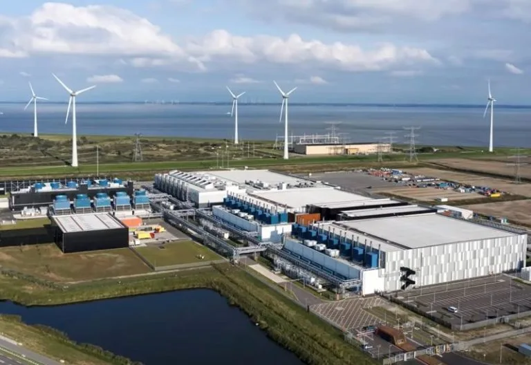
Taiwan Semiconductor Manufacturing Company (TSMC), the world’s premier contract chipmaker, announced new plans to advance its semiconductor fabrication technology with the goal of mastering A12 and A13 process nodes by 2029. The company’s update was revealed during a technology symposium held in the United States that focused on future industry developments.
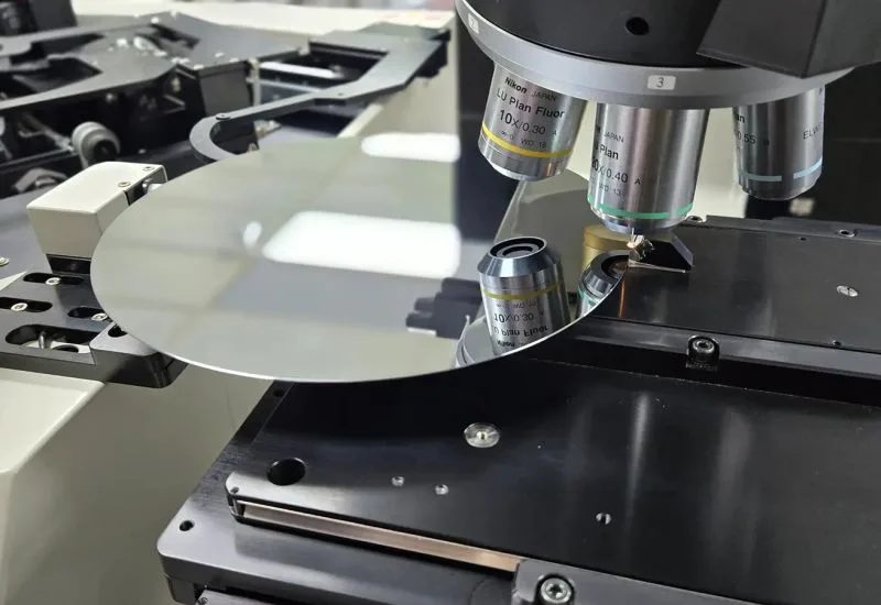
The A12 and A13 process technologies signify a key step forward in the evolution of semiconductor fabrication, representing an approach that will bring TSMC closer to the 1-nanometer scale. Achieving production capability at these scales will enable greater transistor density, efficiency, and performance improvements critical for next-generation chips used across computing, mobile devices, and AI applications.
The semiconductor industry is observing ongoing challenges and intensive innovation as manufacturers seek to push beyond currently established nodes, optimizing their lithography, materials, and design methodologies to realize smaller and more powerful chips. TSMC’s roadmap targeting these sophisticated processes highlights their ambition to remain at the forefront of this competitive landscape.
TSCM’s presentation during the symposium provided glimpses into the company’s strategic focus, which extends well beyond near-term technology nodes. These forward-looking manufacturing capabilities are expected to support client demands for leading-edge chips over the coming decade, although specific technical details, performance metrics, or commercial plans related to A12 and A13 processes have yet to be disclosed.
As one of the industry’s key drivers, TSMC’s progress toward enabling these advanced process technologies will be closely watched by technology companies, equipment suppliers, and analysts aiming to gauge the pace and scale of innovation to meet the growing computational and efficiency demands of future digital ecosystems.
TSMC reveals plans to develop the A12 and A13 chip manufacturing technologies, aiming at near 1-nanometer semiconductor fabrication by 2029.