
Oracle’s Debt Challenges Threaten AI Data Center Project for OpenAI
July 21, 2026
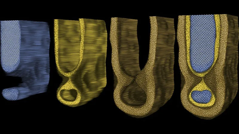
A collaboration between Cornell University and leading semiconductor companies ASM and TSMC has yielded a groundbreaking technology designed to identify hidden atomic-scale defects in advanced semiconductor components. This innovative approach is expected to significantly enhance the debugging and optimization of chip manufacturing processes.
As semiconductor devices continue to shrink to nanometer scales, the challenge of detecting microscopic flaws during fabrication has become more critical. The new visualization tool developed by the research group allows for the precise examination of defects at the scale of just a few atoms. Such granular insight is crucial for fine-tuning production technologies to minimize defects and improve yield rates in high-volume chip manufacturing.
The collaboration draws on the expertise of Cornell University researchers working alongside industrial leaders ASM and TSMC, two well-known entities in the semiconductor manufacturing sector. Their joint effort produced a technique that transcends traditional defect detection methods, offering an unprecedented view into the structural integrity of nanoscale transistors.
This technological advancement is particularly relevant as the semiconductor industry pushes forward with ever-smaller transistor nodes to meet the increasing demands for performance and efficiency in modern electronics. By pinpointing defects at such an atomic scale, manufacturers can more effectively refine and mature their fabrication processes, ultimately driving down the incidence of faulty chips.
While specific technical details and commercial deployment timelines remain closely held, the impact of this development promises to enhance process control and reduce waste in semiconductor production. The ability to visualize and quantify atomic disruptions directly supports the goal of producing highly reliable microelectronic components with minimal defect rates.
This progress aligns with broader industry efforts to innovate inspection and diagnostic tools that maintain Moore’s Law scaling by overcoming physical and engineering limitations inherent in nanoscale device production. The integration of such advanced defect visualization could become a key component in next-generation semiconductor manufacturing workflows.
Overall, this new method represents a significant step forward in the continuous drive to optimize chip fabrication quality, potentially benefiting a wide range of applications from consumer electronics to critical computing infrastructure.
Cornell and industry partners developed a breakthrough method to detect atomic-level defects in advanced semiconductor devices.