Honor Launches X7e Smartphone in Russia Featuring 7200mAh Battery and AI Shortcut Button
July 21, 2026
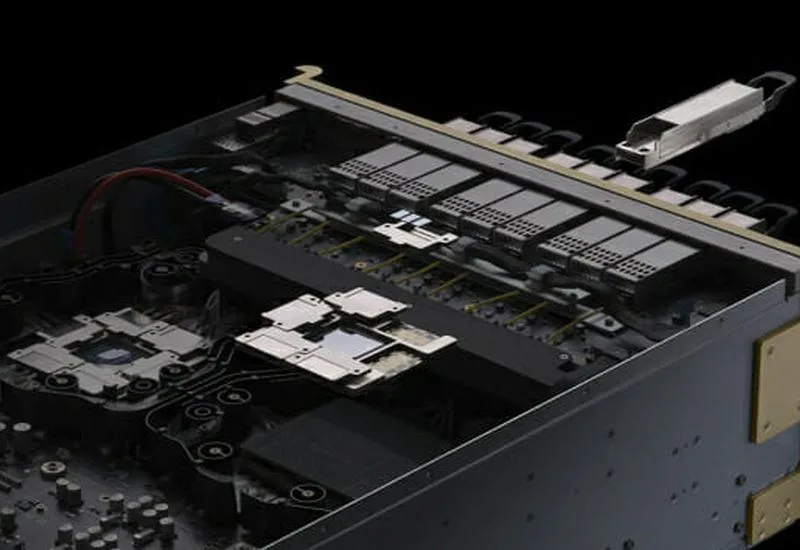
High Bandwidth Memory (HBM) technology, recognized for its vertically stacked chip design, was initially developed to increase memory bandwidth and capacity within limited physical space constraints. However, as accelerator chips demand more memory capacity and higher data throughput than current HBM implementations can provide, memory manufacturers are exploring new architectural approaches.
Traditionally, HBM chips are closely integrated with GPUs through 3D stacking techniques. This physical proximity facilitated exceptional bandwidth gains by minimizing data transmission distances. Despite this advantage, the physical integration also limits how much memory can be added, creating constraints that become increasingly pronounced with modern workloads requiring larger memory pools.
In response to these limitations, industry producers of HBM are considering decoupling the memory physically from the GPU die. This strategy would allow for more flexible scaling of memory capacity without being confined by the current chip package’s spatial restrictions. It represents a shift from the current tightly bound memory-GPU design toward an architecture where memory modules could be expanded independently.
This proposed separation aims to address two central issues in the advancement of GPU memory. Firstly, it offers a pathway to increase overall capacity beyond what can be comfortably stacked vertically in the same package. Secondly, it can potentially sustain or improve the necessary bandwidth by adopting new interconnect technologies to replace the direct TSV (through-silicon via) connections used in stacked designs.
Manufacturers hope that by physically isolating the memory, they can meet the escalating demands of AI accelerators, data center GPUs, and other high-performance computing solutions requiring ever-larger memory resources. Such advancements would allow system designers to enhance configurations with substantial memory upgrades without redesigning the entire GPU chip.
This development signals ongoing innovation in semiconductor packaging and memory technologies to overcome scaling challenges. While details on implementation, standards, or timelines remain forthcoming, the move toward separating HBM from the GPU chip underlines the industry’s pursuit of balancing capacity, bandwidth, and physical form factor to accommodate future computational workloads.
HBM makers aim to decouple memory from GPUs to boost capacity beyond current vertical stacking limits.