Memory Chip Makers Face Potential DRAM Oversupply by 2028 Amid Massive Capacity Expansions
July 20, 2026
The semiconductor industry faces increasingly challenging physical limits as engineers strive to uphold Moore’s Law, the long-standing observation that transistor density on chips doubles approximately every two years. In a recent breakthrough, researchers in the United States have unveiled a pioneering three-dimensional chip stacking approach that significantly outperforms all existing semiconductor density standards.
Traditional attempts at creating 3D-integrated chips have encountered substantial obstacles, chiefly related to thermal management during the manufacturing process. The high temperatures required for bonding multiple layers of semiconductor materials pose considerable risks to chip integrity and performance.
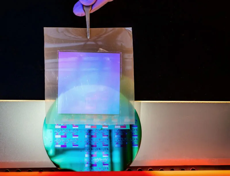
Addressing these constraints, the US research team developed a method that involves stacking ultra-thin silicon membranes resembling layers of an onion. This innovative configuration allows the construction of dense 3D chip structures without exposing the entire assembly to the damaging high temperatures typically involved in conventional processes.
By leveraging these wafer-thin membranes, the technique not only enhances the packing density of transistors dramatically but also sidesteps the thermal limitations that have long hindered stack-based semiconductor integration. The delicate membranes serve as building blocks that can be layered precisely while maintaining the structural and electrical properties essential for reliable chip operation.
This advancement represents a significant leap forward in microelectronics manufacturing, offering a path to prolonging the relevance of Moore’s Law despite the physical and thermal challenges confronting traditional planar chip designs. The approach has the potential to catalyze a new generation of processors and memory devices with dramatically higher performance per unit area compared to contemporary technologies.
While details on the full scope of the manufacturing process, commercial scalability, and timelines for practical deployment were not disclosed, this research marks an important milestone in semiconductor innovation. It highlights the continuing efforts by scientists and engineers to explore three-dimensional architectures as a viable alternative to two-dimensional scaling in the ongoing pursuit of increased computational capability.
As semiconductor demands grow across industries such as artificial intelligence, data centers, and consumer electronics, breakthroughs like this are essential to sustaining the trajectory of technological advancement. Continued research in 3D chip stacking methods will be pivotal in overcoming the fundamental barriers that challenge next-generation semiconductor fabrication.
Researchers in the US demonstrated a novel 3D chip stacking method that surpasses today’s semiconductor density limits while overcoming thermal constraints.