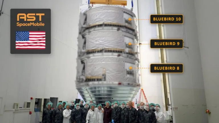
AST SpaceMobile Launches Three BlueBird Satellites Simultaneously, Accelerating Global Internet Ambitions
June 18, 2026

Advances in semiconductor manufacturing continue to face significant challenges, especially when it comes to extreme ultraviolet (EUV) lithography, the cutting-edge process essential for fabricating the most advanced microchips. Recently, a breakthrough from a Japanese scientist promises to make this complex and costly technology more accessible by radically simplifying its optical setup.
Tsumoru Shintake, a professor at the Okinawa Institute of Science and Technology (OIST), has devised an innovative approach to the high numerical aperture (high-NA) EUV lithography systems. His design rethinks the traditional configuration by aligning the key components — the photomask, projection optics, and silicon wafer — along a single linear axis. This contrasts notably with existing industrial EUV scanners, which use more complex arrangements that increase both equipment cost and operational complexity.
This streamlined optical geometry potentially addresses longstanding technical hurdles associated with EUV lithography, such as minimizing aberrations and improving light efficiency. By situating these elements on one line, Shintake’s model could simplify the lithography system architecture substantially, reducing the number of mirrors and optical elements required.
The current high-NA EUV systems involve intricate assemblies to focus extreme ultraviolet light on the photomask and then project the pattern onto a silicon wafer with nanometer precision. Such precision is crucial for creating chips with smaller features, enabling greater performance and energy efficiency. However, these systems come with extremely high production costs, partially due to the complex optics involved.
Implementing the linear design could lead to significant cost reductions in equipment construction and maintenance. While the proposal is still at the research stage, it holds promise for helping chip manufacturers overcome economic and technical barriers related to next-generation lithography processes.
As the semiconductor industry continues to push towards smaller node sizes and increasing chip complexity, simplifying the lithography systems could be a key factor in sustaining Moore’s Law and the advancement of computing technology. The work of Professor Shintake represents an important step toward more affordable and efficient production of leading-edge microchips.
Further development and practical testing of this optical layout will be necessary to validate its commercial viability and integration into existing fabrication lines. Nonetheless, it offers a compelling alternative pathway for refining EUV lithography tools and accelerating innovation in the semiconductor sector.
A new optical design from a Japanese scientist could dramatically reduce expenses in producing advanced chips with EUV lithography.