Caviar Unveils Lionel Messi Edition of Samsung Galaxy Z Fold8 Ultra Ahead of Official Launch
July 17, 2026
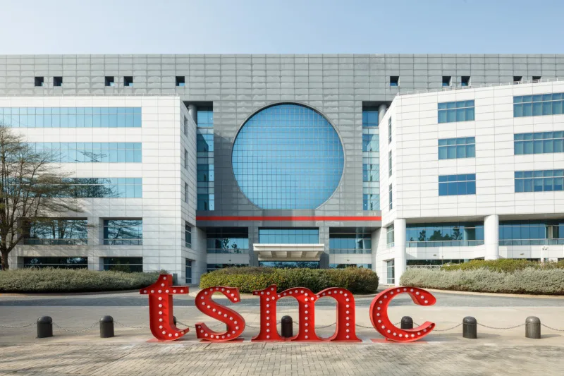
Leading semiconductor manufacturer TSMC has reported significant progress in the development of its advanced 1.4 nanometer process technology, designated A14. The company revealed that the A14 node is advancing at a faster pace than its 2 nanometer N2 process at the same phase of development.
The rapid development of the A14 process comes amid increasing interest from multiple sectors, chiefly smartphone chipset manufacturers, artificial intelligence hardware developers, and companies working on high-performance computing (HPC) solutions. TSMC’s latest update underscores the growing appetite for cutting-edge fabrication technologies capable of delivering efficiency and performance gains critical to these industries.
TSMC’s 1.4 nm A14 node aims to deliver improvements over prior nodes by enabling more complex and energy-efficient chip designs. Though exact technical specifications and release timelines have not been disclosed, the company’s announcement highlights the competitive nature of advanced semiconductor scaling and innovation.
The semiconductor market continues to push the boundaries of miniaturization, with fabrication nodes shrinking to achieve greater transistor densities and power efficiency. TSMC’s positioning of the A14 process ahead of the N2 node in the development cycle may provide a strategic advantage in meeting customer demands sooner.
Given the vital role of semiconductors in powering modern technologies—ranging from consumer electronics to AI workloads and computational research—the evolution of process technologies like A14 will be closely observed by chip designers and industry watchers alike.
Overall, TSMC’s progress report signals robust momentum in its roadmap for next-generation chip manufacturing, reinforcing its status as a frontrunner in the field of semiconductor fabrication.
TSMC reports faster development of its 1.4 nm A14 process compared to the 2 nm N2 node, driven by demand from smartphone and AI chipmakers.