Memory Chip Makers Face Potential DRAM Oversupply by 2028 Amid Massive Capacity Expansions
July 20, 2026
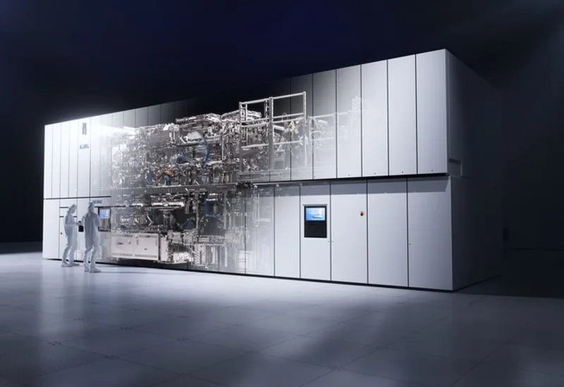
ASML, a prominent supplier of lithography equipment, is advancing towards mass deployment of its cutting-edge High-NA (Numerical Aperture) Extreme Ultraviolet (EUV) lithography technology. This technological leap aims to support semiconductor manufacturers as they push beyond the current limits of chip miniaturization.
In response to the continually shrinking scale of semiconductor components, manufacturers are compelled to adopt more sophisticated production techniques. Conventional EUV tools with lower numerical aperture values have successfully enabled patterning at the nanometer scale, yet the industry now faces increasing challenges in fabricating features thinner than 1.4 nanometers.
High-NA EUV systems represent a significant evolution in lithographic technology, providing markedly improved resolution and image fidelity. This improvement is key to producing the next generation of chips with transistor sizes that fall below the 1.4-nanometer threshold, a milestone considered crucial for sustaining the pace of semiconductor scaling and performance growth.
ASML’s High-NA EUV tools enhance the ability to print smaller and more precise patterns on silicon wafers by increasing the numerical aperture of the imaging system. Essentially, this allows for a higher resolution in the lithography process, supporting finer and more complex circuit designs that were previously unattainable with existing equipment.
The upgrade to High-NA EUV is anticipated to bring transformative benefits to the semiconductor manufacturing ecosystem. It could enable chipmakers to achieve denser transistor arrays, boosting computational power and energy efficiency of future processors and integrated circuits.
According to industry projections, the widespread adoption of High-NA EUV lithography is expected to begin within the next two years, with ASML preparing to deliver these next-generation machines starting next year. The transition marks a pivotal moment, as the technology will underpin production of chips that serve a range of applications from consumer electronics to advanced computing and artificial intelligence.
While precise timing and production volumes were not disclosed, the technological readiness of High-NA EUV machines signals strong momentum within semiconductor manufacturing to overcome the physical and technical constraints associated with continued scaling.
ASML’s advancement is a response to the semiconductor industry’s pressing need to innovate lithographic methods to maintain Moore’s Law and meet evolving demand for higher performance and lower power consumption in electronic devices.
As the High-NA EUV technology moves towards mass implementation, chip manufacturers will gain access to tools that enable the creation of chips with unprecedented levels of miniaturization and complexity, fostering breakthroughs in a broad spectrum of technological fields.
ASML is set to ramp up production of High-NA EUV lithography tools to enable manufacturing of chips thinner than 1.4 nanometers starting next year.