Advancements in CFET Technology Promise Faster, Smaller, and More Reliable Semiconductor Transistors
July 21, 2026

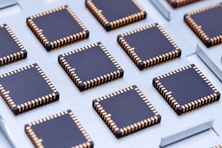
Samsung Electronics has made significant progress in its 2-nanometer semiconductor manufacturing process, increasing the yield of functional chips to over 60%. This marks a substantial improvement compared to the yields reported in the latter half of the previous year, which were below 20%.
The enhanced yield rate is expected to drastically reduce production expenses while enabling Samsung to take on a greater volume of manufacturing orders. Achieving such a high yield in advanced process nodes is critical for maintaining competitiveness in the semiconductor foundry market.
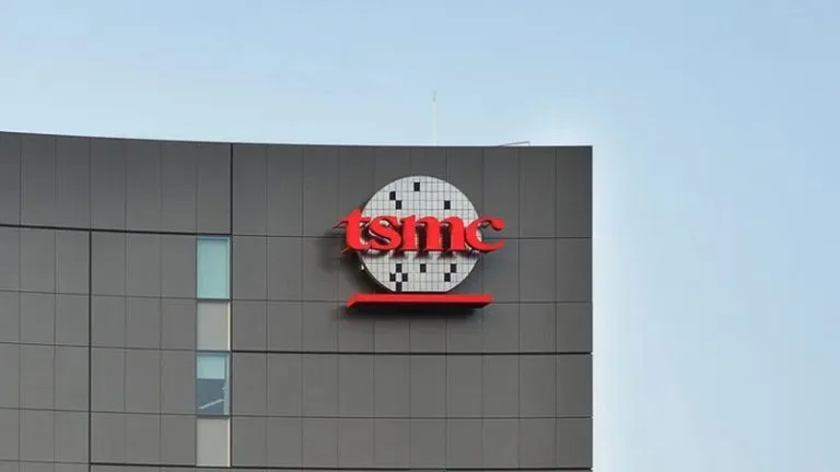
Samsung’s advancements in 2nm technology are a key part of its broader strategy to challenge market leader TSMC. The improved yield indicates that Samsung is closing the gap in process maturity and efficiency, factors that directly impact profitability and customer confidence.
Increasing the yield on cutting-edge semiconductor nodes like 2nm is notoriously difficult due to the complexity of the fabrication process and tight tolerances required. Higher yields translate into more usable chips per production batch, which can make a dramatic difference in supply and cost management.
For Samsung, surpassing the 60% yield threshold means the company can better leverage its manufacturing capacity, attract new clients seeking advanced chip fabrication, and optimize overall operational costs. This progress may influence the competitive dynamics of foundry services, where TSMC has maintained a strong lead.
As semiconductor demand continues to grow across sectors such as mobile devices, high-performance computing, and artificial intelligence, advances in manufacturing yields at the 2nm node could have far-reaching effects. They not only impact the economics of chip production but also the pace at which new technologies reach the market.
While specific details on production volume and customer partnerships were not disclosed, Samsung’s reported yield improvement signals a critical milestone in its ambitions to expand its footprint in the semiconductor foundry industry and compete more closely with long-established players.
Samsung raises yield on its 2-nanometer semiconductor process above 60%, significantly cutting costs and expanding contract manufacturing capacity.